Science > Physics > Semiconductors > PN Junction Diodes
When a crystal of semiconductor is doped such that half the portion of the crystal is doped with a trivalent impurity and the other half is doped with a pentavalent impurity, then the junction (boundary) formed is called a PN junction.
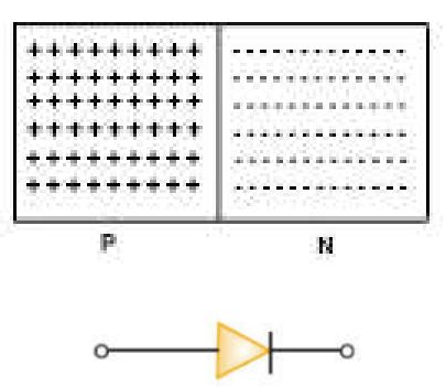
The crystal itself is called a semiconductor diode or a solid-state diode. Due to such doping, one side acts as a p-type semiconductor and the other side acts as an n-type semiconductor.
Depletion Layer and Barrier Potential in PN Junction:
At the ordinary condition, the holes from the p region diffuse into n-region and electron from n- region diffuses into p-region. Thus a thin layer of the positive ion is formed in n-region near the junction and a thin layer of negative ions is formed in p-region near the junction. This thin layer formed near the junction is called the depletion layer or potential barrier
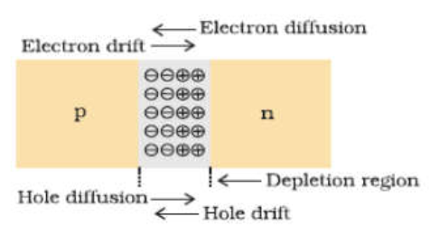
The negative layer on the p-side opposes the further flow of electrons and the positive layer opposes the further flow of holes. The depletion layer has negative potential on the p-side and a positive potential on the n-side which acts as a battery.
Biasing of PN Junction:
Forward Biasing:
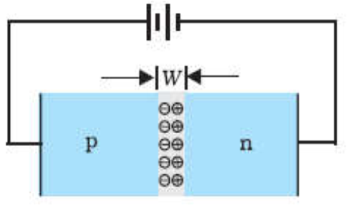
When the p-region of a semiconductor diode is connected to the positive terminal of a battery and the n-region of the semiconductor diode to the negative terminal of a battery then the junction is said to be forward-biased. In this case, the electrons will be pulled towards the positive terminal of the battery and holes towards the negative terminal of the battery and thus electronic current flows in the circuit as shown in the figure.
Reverse Biasing:

Let us consider that the p-region of a semiconductor diode is connected to the negative terminal of a battery and the n-region of semiconductor diode to the positive terminal of a battery then the junction is said to be reverse-biased. In this case, the electrons will be pulled towards the positive terminal of the battery and holes towards the negative terminal of the battery and thus electrons and holes move in the opposite direction away from the junction. Due to the nonavailability of charge carriers, electronic current does not flow in the circuit.
The Use of PN Junction as Diode:
The action of the P-N junction is similar to that of a vacuum diode. It allows the flow of electric current through it when it is forward biased and does not allow the current to flow through it when it is reverse biased. Thus p-n junction allows electric current to flow in one direction only. Thus p-n junction can be used as a rectifier.
A rectifier is electronic device which converts electrical alternating quantity (A.C.) into electrical direct quantity (D.C.)
Use of P-N Junction as Half Wave Rectifier:
A rectifier is electronic device which converts electrical alternating quantity (A.C.) into electrical direct quantity (D.C.) flows in the direction from A to B through load RL.
Circuit Diagram:
The A.C. voltage which is to be rectified is applied across the terminals P1 and P2 of primary of the transformer. The secondary terminals S1 and S2 of the transformer are connected in series with semiconductor diode D and load resistance RL.
Working :
The alternating signal voltage to be rectified is applied across the junction. The alternating signal provides opposite kinds of bias voltage at the junction in each half cycle i.e. if the diode is forward biased in the first half, it is reversed biased in the second half of the cycle.
During the positive half of the input a.c. signal the terminal S1 is positive and terminal S2 is negative, the diode gets forward biased so that the current flows in the direction from A to B through load RL. During the negative half of the input a.c. signal the terminal S1 is negative and terminal S2is positive, the diode gets reverse biased so that there is no flow of current through the load resistance.
Thus, there is a flow of current through RL from A to B during the positive half of a.c. signal only and no current flows during the negative half cycle thus the signal gets rectified. A unidirectional voltage is developed across the output load. As half the input cycle of a.c. signal is used and rectified the arrangement is called a half-wave rectifier.
Graphical Representation:
Variation of A.C. input voltage and D.C. output voltage with time is as shown in the following graphs.
Use of PN Junction as Full Wave Rectifier:
A rectifier is an electronic device which converts electrical alternating quantity (A.C.) into electrical direct quantity (D.C.)
Circuit Diagram:
The A.C. voltage which is to be rectified is applied across the terminals P1 and P2 of primary of a center-tapped transformer.
The secondary terminals S1 and S2 of the transformer are connected to P side of semiconductors diode D1and D2respectively. The n side of the semiconductor diodes is connected together and their common point is connected to center tap through the load resistance RL.
Working :
The alternating signal voltage to be rectified is applied as shown in the circuit diagram. The alternating signal provides opposite kinds of bias voltage at the junction in each half cycle i.e. if the diode is forward biased in the first half, it is reversed biased in the second half of the cycle.
During the positive half of the input a.c. signal the terminal S1 is positive and terminal S2 is negative, the diode D1 gets forward biased and diode D2 gets reverse biased. so that the diode D1 conducts current and the current flows in the direction from A to B through the load RL. During this time the diode D2 remains non conducting.
During the negative half of the input a.c. signal the terminal S1 is negative and terminal S2 is positive, the diode D1gets reverse biased and diode D2 gets forward biased. so that the diode D2 conducts current and the current flows in the direction from A to B through the load RL. During this time the diode D1 remains non-conducting.
Thus, there is a flow of current through RL from A to B during both the half cycles of a.c. signal, thus the signal gets rectified. A unidirectional voltage is developed across the output load. As full input cycle of a.c. signal is used and rectified the arrangement is called a full-wave rectifier.
Graphical Representation:
Variation of A.C. input voltage and D.C. output voltage with time is as shown in the following graphs: